[ad_1]
Billions of tiny transistors supply the processing power in modern smartphones, controlling the flow of electrons with rapid on-and-off switching.
But continual progress in packing more transistors into smaller devices is pushing toward the physical limits of conventional materials. Common inefficiencies in transistor materials cause energy loss that results in heat buildup and shorter battery life, so researchers are in hot pursuit of alternative materials that allow devices to operate more efficiently at lower power.
Now, an experiment conducted at the U.S. Department of Energy’s Lawrence Berkeley National Laboratory (Berkeley Lab) has demonstrated, for the first time, electronic switching in an exotic, ultrathin material that can carry a charge with nearly zero loss at room temperature. Researchers demonstrated this switching when subjecting the material to a low-current electric field.
The team, which was led by researchers at Monash University in Australia and included Berkeley Lab scientists, grew the material from scratch and studied it with X-rays at the Advanced Light Source (ALS), a facility at the U.S. Department of Energy’s Lawrence Berkeley National Laboratory (Berkeley Lab).
The material, known as sodium bismuthide (Na3Bi), is one of two materials that is known to be a “topological Dirac semimetal,” meaning it has unique electronic properties that can be tuned to behave in different ways — in some cases more like a conventional material and in other cases more like a topological material. Its topological properties were first confirmed in earlier experiments at the ALS.
Topological materials are considered promising candidates for next-generation transistors, and for other electronics and computing applications, because of their potential to reduce energy loss and power consumption in devices. These properties can exist at room temperature — an important distinction from superconductors that require extreme chilling — and can persist even when the materials have structural defects and are subject to stress.
Materials with topological properties are the focus of intense research by the global scientific community (see a related article), and in 2016 the Nobel Prize in physics was awarded for theories related to topological properties in materials.
The ease in switching the material studied at the ALS from an electrically conducting state to an insulating, or non-conducting state, bode well for its future transistor applications, said Sung-Kwan Mo, a staff scientist at the ALS who participated in the latest study. The study is detailed in the Dec. 10 edition of the journal Nature.
Another key aspect of the latest study is that the team from Monash University found a way to grow it extremely thin, down to a single layer arranged in a honeycomb pattern of sodium and bismuth atoms, and to control the thickness of each layer they create.
“If you want to make a device, you want to make it thin,” Mo said. “This study proves that it can be done for Na3Bi, and its electrical properties can easily be controlled with low voltage. We are a step closer to a topological transistor.”
Michael Fuhrer, a physicist at Monash University who participated in the study, said, “This discovery is a step in the direction of topological transistors that could transform the world of computation.”
He added, “Ultra-low energy topological electronics are a potential answer to the increasing challenge of energy wasted in modern computing. Information and communications technology already consumes 8 percent of global electricity, and that’s doubling every decade.”
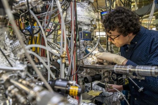
In the latest study, researchers grew the material samples, measuring several millimeters on a side, on a silicon wafer under ultrahigh vacuum at the ALS Beamline 10.0.1 using a process known as molecular beam epitaxy. The beamline allows researchers to grow samples and then conduct experiments under the same vacuum conditions in order to prevent contamination.
This beamline is specialized for an X-ray technique known as angle-resolved photoemission spectroscopy, or ARPES, which provide information about how electrons travel in materials. In typical topological materials, electrons flow around the edges of the material, while the rest of the material serves as an insulator that prevents this flow.
Some X-ray experiments on similar samples were also performed at the Australian Synchrotron to demonstrate the ultrathin Na3Bi was free-standing and did not chemically interact with the silicon wafer it was grown on. Researchers had also studied samples with a scanning tunneling microscope at Monash University that helped to confirm other measurements.
“In these edge paths, electrons can only travel in one direction,” said Mark Edmonds, a physicist at Monash University who led the study. “And this means there can be no ‘back-scattering,’ which is what causes electrical resistance in conventional electrical conductors.”
In this case, researchers found that the ultrathin material became fully conductive when subjected to the electric field, and could also be switched to become an insulator across the entire material when subjected to a slightly higher electric field.
Mo said that the electrically driven switching is an important step to realizing applications for materials — some other research efforts have pursued mechanisms like chemical doping or mechanical strain that are more challenging to control and to perform the switching operation.
The research team is pursuing other samples that can be switched on and off in a similar way to guide the development of a new generation of ultralow-energy electronics, Edmonds said.
The Advanced Light Source is a DOE Office of Science User Facility.
[ad_2]


