[ad_1]
Amid the frenzy of worldwide research on atomically thin materials like graphene, there is one area that has eluded any systematic analysis — even though this information could be crucial to a host of potential applications, including desalination, DNA sequencing, and devices for quantum communications and computation systems.
That missing information has to do with the kinds of minuscule defects, or “holes,” that form in these 2-D sheets when some atoms are missing from the material’s crystal lattice.
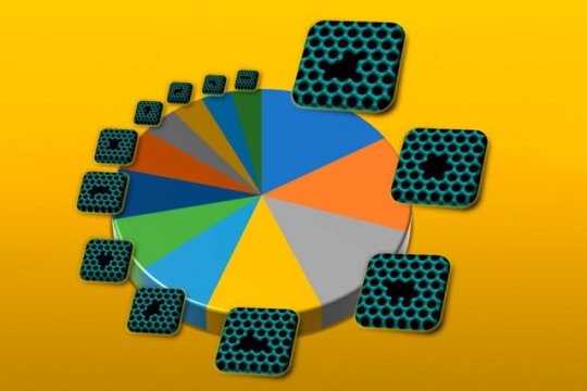
Now that problem has been solved by researchers at MIT, who have produced a catalog of the exact sizes and shapes of holes that would most likely be observed (as opposed to the many more that are theoretically possible) when a given number of atoms is removed from the atomic lattice. The results are described in the journal Nature Materials in a paper by graduate student Ananth Govind Rajan, professors of chemical engineering Daniel Blankschtein and Michael Strano, and four others at MIT, Lockheed Martin Space, and Oxford University.
“It’s been a longstanding problem in the graphene field, what we call the isomer cataloging problem for nanopores,” Strano says. For those who want to use graphene or similar two-dimensional, sheet-like materials for applications including chemical separation or filtration, he says, “we just need to understand the kinds of atomic defects that can occur,” compared to the vastly larger number that are never seen.
For example, Blankschtein points out, by removing just eight contiguous carbon atoms from the hexagonal chicken-wire-like array of atoms in graphene, there are 66 different possible shapes that the resulting hole could have. When the number of atoms removed increases to 12, the number of possible shapes jumps to 3,226, and with 30 atoms removed, there are 400 billion possibilities — a number far beyond any reasonable possibility of simulation and analysis. Yet only a handful of these shapes are actually found in experiments, so the ability to predict which ones really occur could be of great use to researchers.
Describing the lack of information about which kinds of holes actually can form, Strano says, “What that did, practically speaking, is it made a disconnect between what you could simulate with a computer and what you could actually measure in the lab.” This new catalog of the shapes that are actually possible will make the search for materials for specific uses much more manageable, he says.
The ability to do the analysis relied on a number of tools that simply weren’t available previously. “You could not have solved this problem 10 years ago,” Strano says. But now, with the use of tools including chemical graph theory, accurate electronic-structure calculations, and high-resolution scanning transmission electron microscopy, the researchers have captured images of the defects showing the exact positions of the individual atoms.
The team calls these holes in the lattice “antimolecules” and describes them in terms of the shape that would be formed by the atoms that have been removed. This approach provides, for the first time, a simple and coherent framework for describing the whole set of these complex shapes. Previously, “if you were talking about these pores in the material, there was no way to identify” the specific kind of hole involved, Govind Rajan says. “Once people start creating these pores more often, it would be good to have a naming convention” to identify them, he adds.
This new catalog could help to open up a variety of potential applications. “Defects are both good and bad,” Strano explains. “Sometimes you want to prevent them,” because they weaken the material, but “other times you want to create them and control their sizes and shapes,” for example for filtration, chemical processing, or DNA sequencing, where only certain specific molecules can pass through these holes. Another application might be quantum computing or communications devices where holes of a specific size and shape are tuned to emit photons of light of specific colors and energy levels.
In addition to their impact on a material’s mechanical properties, holes affect electronic, magnetic, and optical characteristics as well, Govind Rajan says.
“We think that this work will constitute a valuable tool” for research on defects in 2-D materials, Strano predicts, because it will allow researchers to home in on promising types of defects instead of having to sort through countless theoretically possible shapes “that you don’t care about at all, because they are so improbable they’ll never form.”
[ad_2]


