[ad_1]
A team led by Rutgers University and including scientists from the U.S. Department of Energy’s (DOE) Brookhaven National Laboratory has demonstrated an x-ray imaging technique that could enable the development of smaller, faster, and more robust electronics.
Described in a paper published on Nov. 27 in Nature Communications, the technique addresses a primary limitation in the emerging research field of “spintronics,” or spin electronics, using magnetic materials known as antiferromagnets (AFMs): the ability to image antiphase magnetic domains.
Electrons in magnetic atoms point, or “spin,” in an up or down direction. In all magnetic materials, there are distinct regions — magnetic domains — in which the electron spins are arranged in a regular manner. Several configurations are possible depending on the type of magnetism. In AFMs, the spins on adjacent atoms point in opposite directions (e.g., up-down-up-down). While the spins within each domain are uniformly ordered, those within adjacent domains are aligned in a different way. For example, in AFMs, the spins in one domain may all be arranged in an up-down pattern, while down-up in a neighboring domain. Imaging these “antiphase” domains and the transitions (walls) that exist between them is the first step in being able to manipulate the magnetic state of AFMs to develop spintronic devices.
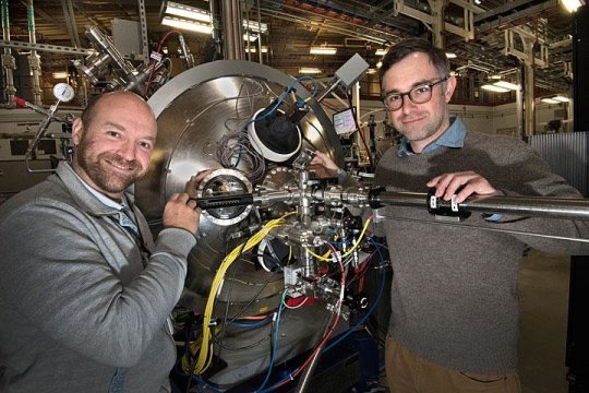
“Ultimately, the goal is to control the number, shape, size, and position of the domains,” said co-author Claudio Mazzoli, lead scientist at the Coherent Soft X-ray Scattering (CSX) beamline at Brookhaven Lab’s National Synchrotron Light Source II (NSLS-II) — a DOE Office of Science User Facility — where the technique was demonstrated. “In general, the electronic properties of domain walls can be different from those in the bulk of the material, and we can take advantage of this fact. Finding a way to control the domains and their walls by external perturbations is key to engineering devices that can efficiently store and process information.”
From charge to spin
Conventional electronics such as computer chips rely on the transport of electrical charge carriers, or electrons, to operate. As these charges move around, they dissipate energy in the form of heat, limiting device efficiency.
Spintronics exploits another intrinsic property of electrons: spin. Because electron spins can be flipped from one magnetic polarity to another much faster than charge can be moved around, devices based on spintronics can be intrinsically faster than today’s electronics.
To date, most spintronic devices have been based on ferromagnets (FMs) — the type of magnets we are most familiar with, as seen on fridges and in computer hard drives. In response to an external magnetic field, the domains in FMs align in a parallel fashion according to the direction of the field.
However, AFMs offer several advantages over FMs. For example, because the spins in AFMs cancel out, these materials have no large-scale magnetism. Thus, their spin orientation can be flipped even faster, and they do not generate stray magnetic fields that can interfere with other sources of magnetization. In addition, they are much more resilient to external magnetic fields.
“Antiferromagnets are intrinsically better protected against losing information through interactions with the environment, including between domains,” explained senior author and Rutgers physics professor Valery Kiryukhin. “Thus, devices based on AFM materials can be made smaller, with information packed more closely together to yield higher storage capacity.”
But the same characteristics that make AFMs appealing for spintronics also make these materials difficult to control.
“In order to control them, we first need to answer very basic questions, such as how the domains are arranged in space and how they and their walls move in response to external perturbations like temperature changes, electric fields, and light pulses,” said Mazzoli.
Antiferromagnetic reflections
In this study, the scientists directed a coherent beam of x-rays from the CSX beamline through a circular pinhole to illuminate the magnetic order of an iron-based AFM sample synthesized by members of Rutgers’ Department of Physics and Astronomy, including Kiryukhin and first author and postdoctoral associate Min Gyu Kim. They set the beamline x-rays to an energy resonating with (close to) the energy of the spins in the material. A detector captured the intensity of the light as it reflected off the sample.
“You can see the scratches on your cell phone screen when light reflects from that surface,” said Mazzoli. “We applied the same kind of principle here but relied on magnetic reflections instead of surface reflections. The magnetic reflections only appear within a very narrow boundary of scattering angles and conditions.”
“Because the incoming beam is coherent — all the photons, or light particles, wave together in an organized fashion — we were able to directly see how two domains are different and how they interfere with one another,” said co-author Mark Dean, a physicist in Brookhaven Lab’s Condensed Matter Physics and Materials Science (CMPMS) Department. “The interference, as revealed in the detector patterns where there is a reduction in signal intensity, told us where the domain boundaries are.”
Though this magnetic diffraction technique is well known, this study represents the first time it has been successfully applied to antiphase domain imaging in AFMs.
“This completely new ability to image antiferromagnetic domain boundaries is only possible because of the superb coherence of the beamline,” said Ian Robinson, X-ray scattering group leader and senior physicist in the CMPMS Department. “The scattering contributions from two antiphase domains are exactly the same in magnitude. They differ only in their phase, which is picked up with coherent x-rays by interference on the detector.”
In fractions of a second, a full picture of extended areas (hundreds of microns by hundreds of microns) of the sample is generated, without having to move any instrumentation. In other magnetic imaging techniques, a probe must be scanned over the surface at multiple points, or calculations are required to project the resulting detector patterns onto real-space images that our eyes can understand.
“We are essentially taking a picture,” said Mazzoli. “The readout of all the pixels in the detector forms a full-field image in a single shot. Images covering even larger millimeter-size areas can be obtained by stitching together multiple images.”
The speed of the technique makes it ideally suited for dynamic experiments. Here, the scientists studied how the magnetic domains changed in real time as they heated the sample to “melt” (remove) its antiferromagnetic order and cooled it to bring back the order in the form of the domain arrangement. They discovered that some of the domains were free to move with each thermal cycle, while others were not.
Going forward, the team plans to test the technique using other AFMs and different classes of materials. The team also plans to improve the current resolution of the technique to below 100 nanometers by reconfiguring the experimental setup. This improved resolution would enable them to determine domain wall thickness.
“To design a spintronic device, you need to know the magnetic configuration of the materials,” said Dean. “Our hope is that we will eventually be able to use this technique to see how magnetism is working in close-to-device conditions.”
The other Brookhaven co-authors are Hu Miao of the CMPMS Department and Andi Barbour, Wen Hu, and Stuart Wilkins of NSLS-II.
The work was supported by DOE’s Office of Science.
[ad_2]


