[ad_1]
To design and improve energy storage materials, smart devices, and many more technologies, researchers need to understand their hidden structure and chemistry. Advanced research techniques, such as ultra-fast electron diffraction imaging can reveal that information. Now, a group of researchers from the U.S. Department of Energy’s (DOE) Brookhaven National Laboratory have developed a new and improved version of electron diffraction at Brookhaven’s Accelerator Test Facility (ATF) — a DOE Office of Science User Facility that offers advanced and unique experimental instrumentation for studying particle acceleration to researchers from all around the world. The researchers published their findings in Scientific Reports, an open-access journal by Nature Research.
Advancing a research technique such as ultra-fast electron diffraction will help future generations of materials scientists to investigate materials and chemical reactions with new precision. Many interesting changes in materials happen extremely quickly and in small spaces, so improved research techniques are necessary to study them for future applications. This new and improved version of electron diffraction offers a stepping stone for improving various electron beam-related research techniques and existing instrumentation.
“We implemented our new focusing system for electron beams and demonstrated that we can improve the resolution significantly when compared to the conventional solenoid technique,” said Xi Yang, author of the study and an accelerator physicist at the National Synchrotron Light Source II (NSLS-II), a DOE Office of Science User Facility at Brookhaven Lab. “The resolution mainly depends on the properties of light — or in our case — of the electron beam. This is universal for all imaging techniques, including light microscopy and x-ray imaging. However, it is much more challenging to focus the charged electrons to a near-parallel pencil-like beam at the sample than it would be with light, because electrons are negatively charged and therefore repulse one another. This is called the space charge effect. By using our new setup, we were able to overcome the space charge effect and obtain diffraction data that is three times brighter and two times sharper; it’s a major leap in resolution.”
Every electron diffraction setup uses an electron beam that is focused on the sample so that the electrons bounce off the atoms in the sample and travel further to the detector behind the sample. The electrons create a so-called diffraction pattern, which can be translated into the structural makeup of the materials at the nanoscale. The advantage of using electrons to image this inner structure of materials is that the so called diffraction limit of electrons is very low, which means scientists can resolve smaller details in the structure compared to other diffraction methods.
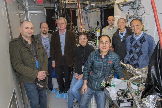
A diverse team of researchers was needed to improve such a complex research method. The Brookhaven Lab team consisted of electron beam experts from the NSLS-II, electron accelerator experts from ATF, and materials science experts from the condensed matter physics & materials science (CMPMS) department.
“This advance would not have been possible without the combination of all our expertise across Brookhaven Lab. At NSLS-II, we have expertise on how to handle the electron beam. The ATF group brought the expertise and capabilities of the electron gun and laser technologies — both of which were needed to create the electron beam in the first place. And the CMPMS group has the sample expertise and, of course, drives the application needs. This is a unique synergy and, together, we were able to show how the resolution of the technique can be improved drastically,” said Li Hua Yu, NSLS-II senior accelerator physicist and co-author of the study.
To achieve its improved resolution, the team developed a different method of focusing the electron beam. Instead of using a conventional approach that involves solenoid magnets, the researchers used two groups of four quadrupole magnets to tune the electron beam. Compared to solenoid magnets, which act as just one lens to shape the beam, the quadrupole magnets work like a specialized lens system for the electrons, and they gave the scientists far more flexibility to tune and shape the beam according to the needs of their experiment.
“Our lens system can provide a wide range of tunability of the beam. We can optimize the most important parameters such as beam size, or charge density, and beam divergence based on the experimental conditions, and therefore provide the best beam quality for the scientific needs,” said Yang.
The team can even adjust the parameters on-the-fly with online optimization tools and correct any nonuniformities of the beam shape; however, to make this measurement possible, the team needed the excellent electron beam that ATF provides. ATF has an electron gun that generates an extremely bright and ultrashort electron beam, which offers the best conditions for electron diffraction.
“The team used a photocathode gun that generates the electrons through a process called photoemission,” said Mikhail Fedurin, an accelerator physicist at ATF. “We shoot an ultrashort laser pulse into a copper cathode, and when the pulse hits the cathode a cloud of electrons forms over the copper. We pull the electrons away using an electric field and then accelerate them. The amount of electrons in one of these pulses and our capability to accelerate them to specific energies make our system attractive for material science research — particularly for ultrafast electron diffraction.”
The focusing system together with the ATF electron beam is very sensitive, so the researchers can measure the influences of Earth’ magnetic field on the electron beam.
“In general, electrons are always influenced by magnetic fields — this is how we steer them in particle accelerators in the first place; however, the effect of Earth’s magnetic field is not negligible for the low-energy beam we used in this experiment,” said Victor Smalyuk, NSLS-II accelerator physics group leader and co-author of the study. “The beam deviated from the desired trajectory, which created difficulties during the initial starting phase, so we had to correct for this effect.”
Beyond the high brightness of the electron beam and the high precision of the focusing system, the team also needed the right sample to make these measurements. The CMPMS group provided the team with a polycrystalline gold film to fully explore the newly designed lens system and to put it to the test.
“We made the sample by depositing the gold atoms on a several nanometer thick carbon film using a technique called thermal evaporation,” said Junjie Li, a physicist in the CMPMS department. “We evaporated gold particles so that they condense on the carbon film and form tiny, isolated nanoparticles that slowly merge together and form the polycrystalline film.”
This film was essential for the measurements because it has randomly oriented crystals that merge together. Therefore, the inner structure of the sample is not uniform, but consists of many differently oriented areas, which means that the diffraction pattern mainly depends on the electron beam qualities. This gives the scientists the best ground to really test their lens system, to tune the beam, and to see the impact of their tuning directly in the quality of the diffraction measurement.
“We initially set out to improve electron diffraction for scientific studies of materials, but we also found that this technique can help us characterize our electron beam. In fact, diffraction is very sensitive to the electron beam parameters, so we can use the diffraction pattern of a known sample to measure our beam parameters precisely and directly, which is usually not that easy,” said Yang.
The team intends to pursue further improvements, and they already have plans to develop another setup for ultra-fast electron microscopy to directly visualize a biological sample.
“We hope to achieve ultrafast single-shot electron beam imaging at some point and maybe even make molecular movies, which isn’t possible with our current electron beam imaging setup,” said Yang.
[ad_2]


