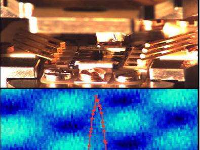
It images single atoms. It maps atomic-scale hills and valleys on metal and insulating surfaces. And it records the flow of current across atom-thin materials subject to giant magnetic fields. Scientists at the National Institute of Standards and Technology (NIST) have developed a novel instrument that can make three kinds of atom-scale measurements simultaneously. Together, these measurements can uncover new knowledge about a wide range of special materials that are crucial for developing the next generation of quantum computers, communications and a host of other applications.
From smartphones to multicookers, devices that perform several functions are often more convenient and potentially less expensive than the single-purpose tools they replace, and their multiple functions often work better in concert than separately. The new three-in-one instrument is a kind of Swiss Army knife for atom-scale measurements. NIST researcher Joseph Stroscio and his colleagues, including Johannes Schwenk and Sungmin Kim, present a detailed recipe for building the device in the Review of Scientific Instruments.
“We describe a blueprint for other people to copy,” Stroscio said. “They can modify the instruments they have; they don’t have to buy new equipment.”
By simultaneously conducting measurements on scales ranging from nanometers to millimeters, the instrument can help researchers zero in on the atomic origins of several unusual properties in materials that may prove invaluable for a new generation of computers and communication devices. These properties include the resistance-less flow of electric current, quantum jumps in electrical resistance that could serve as novel electrical switches, and new methods to design quantum bits, which could lead to solid-state-based quantum computers.
“By connecting the atomic with the large scale, we can characterize materials in a way that we couldn’t before,” said Stroscio.
Although the properties of all substances have their roots in quantum mechanics — the physical laws that govern the Lilliputian realm of atoms and electrons — quantum effects can often be ignored on large scales such as the macroscopic world we experience every day. But for a highly promising class of materials known as quantum materials, which typically consist of one or more atomically thin layers, strong quantum effects between groups of electrons persist over large distances and the rules of quantum theory can dominate even on macroscopic length scales. These effects lead to remarkable properties that can be harnessed for new technologies.
To study these properties more precisely, Stroscio and his colleagues combined in a single instrument a trio of precision measuring devices. Two of the devices, an atomic force microscope (AFM) and a scanning tunneling microscope (STM), examine microscopic properties of solids, while the third tool records the macroscopic property of magnetic transport — the flow of current in the presence of a magnetic field.
“No single type of measurement provides all the answers for understanding quantum materials,” said NIST researcher Nikolai Zhitenev. “This device, with multiple measuring tools, provides a more comprehensive picture of these materials.”
To build the instrument, the NIST team designed an AFM and a magnetic-transport-measuring device that were more compact and had fewer moving parts than previous versions. They then integrated the tools with an existing STM.
Both an STM and an AFM use a needle-sharp tip to examine the atomic-scale structure of surfaces. An STM maps the topography of metal surfaces by placing the tip within a fraction of a nanometer (billionth of a meter) of the material under study. By measuring the flow of electrons that tunnels out of the metal surface as the sharp tip hovers just above the material, the STM reveals the sample’s atomic-scale hills and valleys.
In contrast, an AFM measures forces by changes in the frequency at which its tip oscillates as it hovers over a surface. (The tip is mounted on a miniature cantilever, which allows the probe to swing freely.) The oscillation frequency shifts as the sharp probe senses forces, such as the attraction between molecules, or the electrostatic forces with the material’s surface. To measure magnetic transport, a current is applied across a surface immersed in a known magnetic field. A voltmeter records the voltage at different places on the device, revealing the electrical resistance of the material.
The ensemble is mounted inside a cryostat, a device that chills the system to one-hundredth of a degree above absolute zero. At that temperature, the random quantum jitter of atomic particles is minimized and large-scale quantum effects become more pronounced and easier to measure. The three-in-one device, which is shielded from external electrical noise, is also five to 10 times more sensitive than any previous set of similar instruments, approaching the fundamental quantum noise limit that can be achieved at low temperatures.
Although it’s possible for three entirely independent instruments — an STM, an AFM and a magnetic transport setup — to make the same measurements, inserting and then retracting each tool can disturb the sample and diminish the accuracy of the analysis. Separate instruments can also make it difficult to replicate the exact conditions, such as the temperature and rotation angle between each ultrathin layer of the quantum material, under which previous measurements were made.
To achieve the goal of a three-in-one instrument with high sensitivity, the NIST team partnered with an international team of experts, including Franz Giessibl from the University of Regensburg, Germany, who invented a highly effective AFM known as the qPlus AFM. The team chose a compact design that increased the stiffness of the microscope and outfitted the system with a series of filters to screen out radio frequency noise. The atomically thin needle of the STM doubled as the force sensor for the AFM, which was based on a new force sensor design created by Giessibl for the three-in-one instrument.
For Stroscio, a pioneer in building ever-more-sophisticated STMs, the new device is something of a pinnacle in a more than three-decade career in scanning probe microscopy. His team, he noted, had been struggling for several years to dramatically reduce the electrical noise in its measurements. “We have now achieved the ultimate resolution given by thermal and quantum limits in this new instrument,” Stroscio said.
“This feels like I’ve climbed the highest peak of the Rocky Mountains,” he added. “It’s a nice synthesis of everything I’ve learned over the last 30-plus years.”


