[ad_1]
Even solar cells made of a perfect miracle material would never be able to convert 100 % of sunlight to electrical energy. This is because the theoretical maximum achievable power is limited by the position of the energy bands of the electrons, and by unavoidable radiation of photons (the thermodynamic or Shockley-Queisser limit). Maximum power conversion efficiency for silicon is about 33 %, for example. But even this value will never actually be reached. This is due to defects of various kinds causing the loss of some of the charge carriers released by sunlight. In order to approach the maximum value, it is therefore necessary to investigate the various defects in solar cells and determine which ones lead to losses and how.
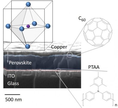
Organometallic perovskite absorber layers are regarded as a particularly exciting new material class for solar cells — in just ten years, their efficiency has increased from three per cent to over twenty per cent, an amazing success story. Now a team headed by Prof. Dr. Dieter Neher at the University of Potsdam and Dr. Thomas Unold at HZB has succeeded in identifying the decisive loss processes in perovskite solar cells that limit the efficiency.
At certain defects in the crystal lattice of the perovskite layer, charge carriers (i.e. electrons and “holes”) that have just been released by sunlight can recombine again and thus be lost. But whether these defects were preferentially located within the perovskite layer, or instead at the interface between the perovskite layer and the transport layer was unclear until now.
To determine this, the scientists employed photoluminescence techniques with high precision, spatial and temporal resolution. Using laser light, they excited the square-centimetre-sized perovskite layer and detected where and when the material emitted light in response to the excitation. “This measurement method at our lab is so precise, we can determine the exact number of photons that have been emitted,” explains Unold. And not only that, the energy of the emitted photons was precisely recorded and analyzed as well using a hyperspectral CCD camera.
“In this way, we were able to calculate the losses at every point of the cell and thereby determine that the most harmful defects are located at the interfaces between the perovskite absorber layer and the chargetransport layers,” reports Unold. This is important information for further improving perovskite solar cells, for instance by means of intermediate layers that have a positive effect or through modified fabrication methods.
With the help of these findings, the group led by Prof. Dr. Dieter Neher and Dr. Martin Stolterfoht at the University of Potsdam has succeeded in reducing interfacial recombination and thus increasing the efficiency of 1cm2sized perovskite solar cells to well over 20 %.
Story Source:
Materials provided by Helmholtz-Zentrum Berlin für Materialien und Energie. Note: Content may be edited for style and length.
[ad_2]


