[ad_1]
Researchers have developed a revolutionary method to ‘print’ large-scale sheets of two dimensional piezoelectric material, opening new opportunities for piezo-sensors and energy harvesting.
Importantly, the inexpensive process allows the integration of piezoelectric components directly onto silicon chips.
Until now, no 2D piezoelectric material has been manufactured in large sheets, making it impossible to integrate into silicon chips or use in large-scale surface manufacturing.
This limitation meant that piezo accelerometer devices — such as vehicle air bag triggers or the devices that recognise orientation changes in mobile phones — have required separate, expensive components to be embedded onto silicon substrates, adding significant manufacturing costs.
Now, FLEET researchers at RMIT University in Melbourne have demonstrated a method to produce large-scale 2D gallium phosphate sheets, allowing this material to be formed at large scales in low-cost, low-temperature manufacturing processes onto silicon substrates, or any other surface.
Gallium phosphate (GaPO4) is an important piezoelectric material commonly used in pressure sensors and microgram-scale mass measurement, particularly in high temperatures or other harsh environments.
“As so often in science, this work builds on past successes,” lead researcher Professor Kourosh Kalantar-zadeh explains. “We adopted the liquid-metal material deposition technique we developed recently to create 2D films of GaPO4 through an easy, two-step process.”
Professor Kalantar-zadeh, now Professor of Chemical Engineering at UNSW, led the team that developed the new method while Professor of Electronic Engineering at RMIT University. The work was materialised as a result of significant contribution from RMIT’s Dr Torben Daeneke and extreme persistence and focus shown by the first author of the work, PhD researcher Nitu Syed.
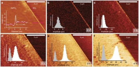
The revolutionary new method allows easy, inexpensive growth of large-area (several centimetres), wide-bandgap, 2D GaPO4 nanosheets of unit cell thickness.
It is the first demonstration of strong, out-of-plane piezoelectricity of the popular piezoelectric material.
THE TWO-STEP PROCESS
- Exfoliate self-limiting gallium oxide from the surface of liquid gallium made possible by the lack of affinity between oxide and the bulk of the liquid metal
- ‘Print’ that film onto a substrate and transform it into 2D GaPO4 via exposure to phosphate vapour.
APPLICATIONS
The new process is simple, scalable, low-temperature and cost effective, significantly expanding the range of materials available to industry at such scales and quality.
The process is suitable for the synthesis of free standing GaPO4 nanosheets. The low temperature synthesis method is compatible with a variety of electronic device fabrication procedures, providing a route for the development of future 2D piezoelectric materials.
This simple, industry-compatible procedure to print large surface area 2D piezoelectric films onto any substrate offers tremendous opportunities for the development of piezo-sensors and energy harvesters.
PIEZOELECTRIC MATERIALS
These are materials that can convert applied mechanical force or strain into electrical energy. Such materials form the basis of sound and pressure sensors, embedded devices that are powered by vibration or bending, and even the simple ‘piezo’ lighter used for gas BBQs and stovetops.
Piezoelectric materials can also take advantage of the small voltages generated by tiny mechanical displacement, vibration, bending or stretching to power miniaturised devices.
THE MATERIAL: GALLIUM PHOSPHATE (GaPO4)
Gallium phosphate is a quartz-like crystal used in piezoelectric applications such as pressure sensors since the late 1980s, and particularly valued in high-temperature applications. Because it does not naturally crystallise in a stratified structure and hence cannot be exfoliated using conventional methods, its use to date has been limited to applications that rely on carving the crystal from its bulk.
[ad_2]


