[ad_1]
A team of scientists working at the Department of Energy’s Lawrence Berkeley National Laboratory (Berkeley Lab) has confirmed a special property known as “chirality” — which potentially could be exploited to transmit and store data in a new way — in nanometers-thick samples of multilayer materials that have a disordered structure.
While most electronic devices rely on the flow of electrons’ charge, the scientific community is feverishly searching for new ways to revolutionize electronics by designing materials and methods to control other inherent electron traits, such as their orbits around atoms and their spin, which can be thought of as a compass needle tuned to face in different directions.
These properties, scientists hope, can enable faster, smaller, and more reliable data storage by facilitating spintronics — one facet of which is the use of spin current to manipulate domains and domain walls. Spintronics-driven devices could generate less heat and require less power than conventional devices.
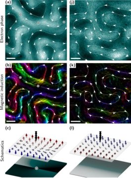
In the latest study, detailed in the May 23 online edition of the journal Advanced Materials, scientists working at Berkeley Lab’s Molecular Foundry and Advanced Light Source (ALS) confirmed a chirality, or handedness, in the transition regions — called domain walls — between neighboring magnetic domains that have opposite spins.
Scientists hope to control chirality — analogous to right-handedness or left-handedness — to control magnetic domains and convey zeros and ones as in conventional computer memory.
The samples were composed of an amorphous alloy of gadolinium and cobalt, sandwiched between ultrathin layers of platinum and iridium, which are known to strongly impact neighboring spins.
Modern computer circuits commonly use silicon wafers based on a crystalline form of silicon, which has a regularly ordered structure. In this latest study, the material samples used in experiments were amorphous, or noncrystalline, which means their atomic structure was disordered.
Experiments revealed a dominant chirality in the magnetic properties of these domain walls that could possibly be flipped to its opposite. Such a flipping mechanism is a critical enabling technology for spintronics and variant fields of research that are based on the electron’s spin property.
The science team worked to identify the right thickness, concentration, and layering of elements, and other factors to optimize this chiral effect.
“Now we have proof that we can have chiral magnetism in amorphous thin films, which no one had shown before,” said Robert Streubel, the study’s lead author and a postdoctoral researcher in Berkeley Lab’s Materials Sciences Division. The success of the experiments, he said, opens the possibility of controlling some properties of domain walls, such as chirality, with temperature, and of switching a material’s chiral properties with light.
Amorphous materials, despite their disordered structure, could also be manufactured to overcome some of the limitations of crystalline materials for spintronics applications, Streubel noted. “We wanted to investigate these more complex materials that are easier to make, especially for industrial applications.”
The research team enlisted a unique, high-resolution electron microscopy technique at Berkeley Lab’s Molecular Foundry, and conducted the experiments in a so-called Lorentz observation mode to image the magnetic properties of the material samples. They combined these results with those of an X-ray technique at the ALS known as magnetic circular dichroism spectroscopy to confirm the nanoscale magnetic chirality in the samples.
The Lorentz microscopy technique employed at the Molecular Foundry’s National Center for Electron Microscopy provided the tens-of-nanometers resolution required to resolve the magnetic domain properties known as spin textures.
“This high spatial resolution at this instrument allowed us to see the chirality in the domain walls — and we looked through the whole stack of materials,” said Peter Fischer, a co-leader of the study and a senior staff scientist in the Lab’s Materials Sciences Division.
Fischer noted that the increasingly precise, high-resolution experimental techniques — which use electron beams and X-rays, for example — now allow scientists to explore complex materials that lack a well-defined structure.
“We are now looking with new kinds of probes,” he said, that are drilling down to ever-smaller scales. “Novel properties and discoveries can quite often occur at materials’ interfaces, which is why we ask: What happens when you put one layer next to another? And how does that impact the spin textures, which are a material’s magnetic landscapes of spin orientations?”
The ultimate research tool, Fischer said, which is on the horizon with the next-generation of electron and X-ray probes, would provide scientists the capability to see directly, at atomic resolution, the magnetic switching occurring in a material’s interfaces at femtosecond (quadrillionths of a second) timescales.
“Our next step is therefore to go into the dynamics of the chirality of these domain walls in an amorphous system: to image these domain walls while they’re moving, and to see how atoms are assembled together,” he said.
Streubel added, “It was really a profound study in almost every aspect that was needed. Every piece by itself posed challenges.” The Lorentz microscopy results were fed into a mathematical algorithm, customized by Streubel, to identify domain wall types and chirality. Another challenge was in optimizing the sample growth to achieve the chiral effects using a conventional technique known as sputtering.
The algorithm, and the experimental techniques, can now be applied to a whole set of sample materials in future studies, and “should be generalizable to different materials for different purposes,” he said.
The research team also hopes that their work may help drive R&D related to spin orbitronics, where “topologically protected” (stable and resilient) spin textures called skyrmions could potentially replace the propagation of tiny domain walls in a material and lead to smaller and faster computing devices with lower power consumption than conventional devices.
[ad_2]


