[ad_1]
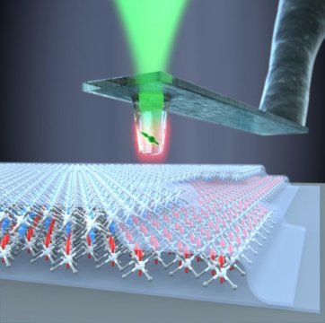
For the first time, physicists at the University of Basel have succeeded in measuring the magnetic properties of atomically thin van der Waals materials on the nanoscale. They used diamond quantum sensors to determine the strength of the magnetization of individual atomic layers of the material chromium triiodide. In addition, they found a long-sought explanation for the unusual magnetic properties of the material. The journal Science has published the findings.
The use of atomically thin, two-dimensional van der Waals materials promises innovations in numerous fields in science and technology. Scientists around the world are constantly exploring new ways to stack different single atomic layers and thus engineer new materials with unique, emerging properties.
These super-thin composite materials are held together by van der Waals forces and often behave differently to bulk crystals of the same material. Atomically thin van der Waals materials include insulators, semiconductors, superconductors and a few materials with magnetic properties. Their use in spintronics or ultra-compact magnetic memory media is highly promising.
The first quantitative measurement of magnetization
Until now, it has not been possible to determine the strength, alignment and structure of these magnets quantitatively nor on the nanoscale. The team headed by Georg-H.-Endress Professor Patrick Maletinsky from the Department of Physics and the Swiss Nanoscience Institute at the University of Basel have demonstrated that the use of diamond tips decorated with single electron spins in an atomic force microscope is ideally suited to these types of studies.
“Our method, which uses the individual spins in diamond color centers as sensors, opens up a whole new field. The magnetic properties of two-dimensional materials can now be studied on the nanoscale and even in a quantitative manner. Our innovative quantum sensors are perfectly suited to this complex task,” says Maletinsky.
The number of layers is critical
Using this technology which was originally developed in Basel and which is based on a single electron spin, the scientists collaborated with researchers from the University of Geneva to determine the magnetic properties of single atomic layers of chromium triiodide (CrI3). The researchers were thus able to find the answer to a key scientific question about the magnetism of this material.
As a three-dimensional, bulk crystal, chromium triiodide is fully magnetically ordered. In the case of few atomic layers, however, only stacks with an odd number of atomic layers show a non-zero magnetization. Stacks with an even number of layers exhibit an antiferromagnetic behavior; i.e. they are not magnetized. The cause of this “even/odd-effect” and the discrepancy to bulk material was previously unknown.
Strain as the cause
Maletinsky’s team was able to demonstrate that this phenomenon is due to the specific atomic arrangement of the layers. During sample preparation, the individual chromium triiodide layers slightly move against one another. The resulting strain in the lattice means the spins of successive layers are unable to align in the same direction; instead, the spin direction alternates in the layers. With an even number of layers, the magnetization of the layers cancel out; with an odd number, the strength of the measured magnetization corresponds to that of a single layer.
However, when the strain in the stack is released — for example, by puncturing the sample — the spins of all layers can align in the same direction, as is also observed in bulk crystals. The magnetic strength of the entire stack is then consistent with the sum of the individual layers.
The work conducted by the Basel scientists thereby not only answers a key question about two-dimensional van der Waals magnets, it also opens interesting perspectives on how their innovative quantum sensors can be used in the future to study two-dimensional magnets in order to contribute to the development of novel electronic components.
Story Source:
Materials provided by University of Basel. Note: Content may be edited for style and length.
[ad_2]


