[ad_1]
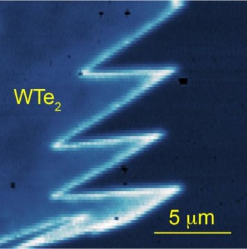
A research team at the University of California, Riverside, and the University of Washington has for the first time directly imaged “edge conduction” in monolayer tungsten ditelluride, or WTe2, a newly discovered 2-D topological insulator and quantum material.
The research makes it possible to exploit this edge conduction feature to build more energy-efficient electronic devices.
In a typical conductor, electrical current flows everywhere. Insulators, on the other hand, do not readily conduct electricity. In topological insulators, a special type of material, the interior works as an insulator, but the boundaries of such materials are guaranteed to be conductive due to its topological property, resulting in a feature called “topological edge conduction.”
Topology is the mathematical study of the properties of a geometric figure or solid that is unchanged by stretching or bending. Applying this concept to electronic materials leads to discoveries of many interesting phenomena, including topological edge conduction. Working like highways for electrons, channels of topological edge conduction allow electrons to travel with little resistance. Further, because edge channels can be potentially very narrow, electronic devices can be further miniaturized.
Study results appear today in Science Advances.
“Several materials have been shown to be 3-D topological insulators,” said Yongtao Cui, an assistant professor of physics and astronomy at UCR, who led the research. “But 2-D topological insulators are rare. Several recent experiments established that monolayer WTe2 is the first atomically thin 2-D topological insulator.”
Cui explained that for a 3-D topological insulator, conduction appears at its surfaces; for a 2-D sheet-like material, such conducting features are simply at the edges of the sheet.
Cui’s lab used a novel experimental technique called Microwave Impedance Microscopy, or MIM, to directly image the conduction at the edges of monolayer WTe2.
“Our results unambiguously confirm edge conduction in this promising material,” Cui said.
Although WTe2 has been known to exist for decades, interest in this material got a boost in only the last few years due to its exotic physical and electronic properties discovered using topological physics. WTe2 layers are stacked together via van der Waals interactions and can be easily exfoliated into thin, 2-D, graphene-like sheets.
“In addition to conduction at the edges in monolayer WTe2, we also found that the conductive channels can extend to the interior of the material, due to imperfections — such as cracks,” Cui said. “Our observations point to new ways to control and engineer such conduction channels via mechanical or chemical means.”
Cui’s collaborators at the University of Washington prepared the monolayer WTe2 samples. At UCR, his lab performed the MIM measurement, which involved sending a microwave electrical signal to a sharp metal tip, and positioning the tip near the surface of monolayer WTe2. By resolving the microwave signal bounced back by the sample, the researchers could determine whether the sample region directly below the tip was conductive or not.
“We scanned the tip across the entire sample and directly mapped the local conductivity,” Cui said. “We performed all the measurements at cryogenic temperatures, needed for monolayer WTe2 to exhibit the topological property. The topological properties of monolayer WTe2 can potentially serve as a platform to realize essential operations in quantum computing.”
Cui’s lab is already exploring new ways to manipulate the edge conduction channels and topological physics in monolayer WTe2.
“We are looking into whether stacking monolayer WTe2 with other 2-D materials can alter its topological property,” he said. “We are also using mechanical and chemical methods to create networks of conduction channels. The MIM technique we used offers a powerful means to characterize the conduction channels in topological materials such as monolayer WTe2.”
Cui was joined in the study by Yanmeng Shi, Ben Niu, and Brian A. Francisco of UCR; Joshua Kahn, Zaiyao Fei, Bosong Sun, Xinghan Cai, Xiaodong Xu, and David H. Cobden of the University of Washington; Di Wu of Nanjing University, China; and Zhi-Xun Shen of Stanford University; Shi, Kahn, and Niu are co-first authors of the research paper.
The work done at UCR was supported by Cui’s startup funds.
[ad_2]


